PICnMIX
February 2, 2009 last updated. Notesand pictures re "Bonus" Version "B" PnM added
This is the PICnMIX pcb version by VK3PE & C.S.
Please check Errors below for Panel #1 PnM only ! Nov 2007, Jan 2008.
Quite a few pictures, so may take a while to load.
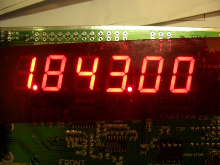
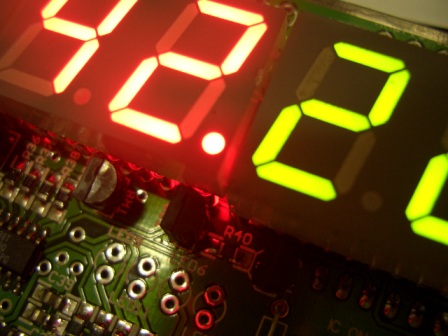
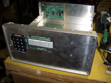
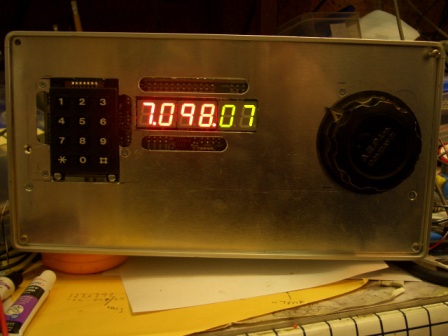
Here are some pictures of my build up of the panel #1 PnM PCB. The display section PCB shown is on the 1.843MHz AM net frequency used in Melbourne.
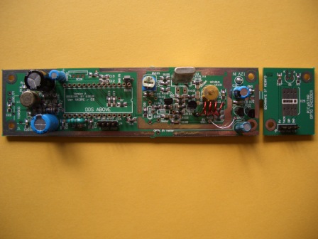
PICnMIX is in 2 parts. The 2nd PCB (further down page) contains the Butler oscillator, amplifier and Opto sensor which can be separated if required. I have used 0805 sized SMD resistors and capacitors but 1206 or even 0603 can be used in most places.
Above the display, is a row of holes for the S'meter, Atten, DSP and IP3 LED's. The LED's for VFO etc are below the display and again not fitted as they are best fitted later when the front panel is assembled.
I tried a few different displays. The displays used here were Avago (HP) HDSP-K121 0.56", high efficiency, low current types. See below for use of normal current Red & Green displays.
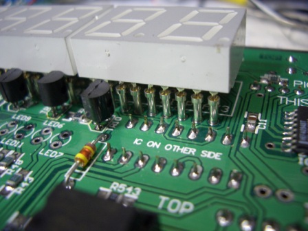
NOTE: the 6 BC327's under the display are shown incorrectly on the PCB's component overlay fopr Panel #1 PnM only.
They should be inserted opposite to what is shown on the PCB overlay! ie. The printed outline. The pictures below are CORRECT.
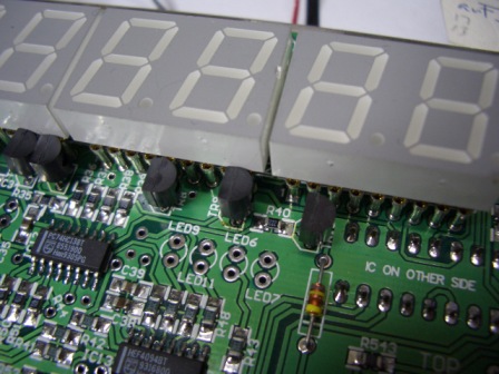
Note also the use of turned pins removed from a turned pin socket to mount the displays. These space the displays up to a more suitable level, compatible with the rest of the assembly.
(, On the "bonus" PnM PCB on Panel #2, the overlay is correct)
21st July, 2008 The PnM boards marked Version "B" on panel #2 have been CORRECTED. You can fit the BC327's as per the PCB overlay.
 Version "B"
5th Nov..... Error !
The text "15MHz" on this board should be "5MHz" (corrected on "Bonus" PnM PCB on panel #2)
G4IZS has identified two potential ground problems on the display board:- (corrected on "Bonus" PnM PCB on panel #2)
1) C35 adjacent to LED8 has no ground. Link a resistor wire offcut from C35 (near "IC12" text) to top of LED8 near the "R35" text.
2) Pin 19 of the PIC (IC3) should be linked across to pin 8, which is below it and to the right, just above the text "C30"
Refer to this pdf file for details.
26th NOV Butler heater transistor should be TIP122, not TIP123.
Display types.
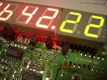
I have now tried 3 types of display in this Board. (24th Oct 2007) All were bought from Farnell. Standard brightness are fine, as is the green type although, as expected, brightness is lower but quite OK. The picture below still has the low current ones fitted but you can also see the green displays.
There is a point to watch here though. The standard brightness and green displays are slightly higher/taller. You need to seat the BC327's well down on the PCB to make sure they clear the displays. Or, when you fit them, put the displays in first, then angle the BC327's away from the displays slightly. (Neither has been done in the pictures) The left picture is not 100% clear, but you can just see that the green display (appears yellow, but is actually green) is taller than the red low current type type. The standard type displays are also taller. See how close the BC327's are.
 Farnell
numbers here:
Farnell
numbers here:
RED std type HDSP-521E 100-3314
Green std type HDSP-521G 100-3316
Please double check numbers before ordering though !!!!
BUTLER Section
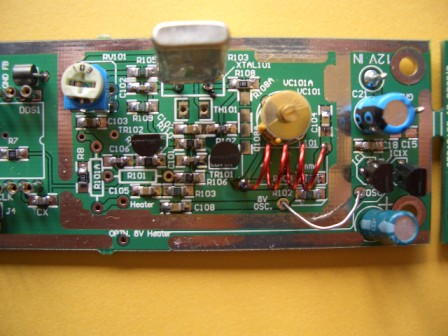
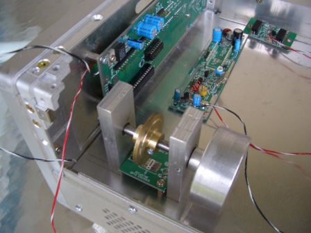
This is my Butler board assembly. I found that the Butler would oscillate without the crystal inserted. I could tune it from about 120-180MHz. There are Posts about this on the Yahoo group and the fix is to lower the value of R104 (R4 in original documentation) I simply placed a 270R across R104 and it was fixed. Heater transistor etc yet to be fitted. I have used 0805 parts mainly but you will notice a few smaller, 0603, parts used also.
I elected to fit both 78L08 regulators. Later, a PCB shield will be fitted around the oscillaotr section and two feedthrough caps. will be fitted. On eon the right for the oscillator power, another at the bottom, near R101A, for the heater power. Connect the cap to "heater" and "optn 8v heater" pads.
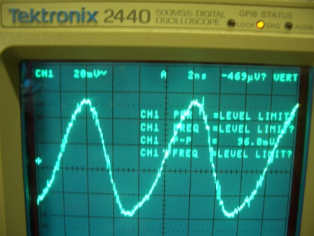
This is the output of my 122.3MHz crystal. (Using x10 probe) NOTE your frequency will depend on the crystal used.
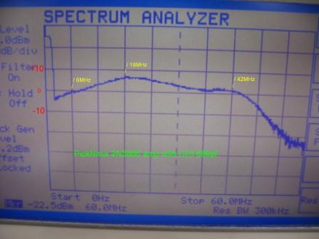
Testing the 2N3866 stage with Low Pass Filter:-
After finding a dud 2N3866 that I used from the "junk box", I replaced it with a 2N5109. I then swept the low pass filter and amplifier stage. This is the result. It does roll off a little earlier than the specified 42MHz, which may affect the injection level available at the top end of 10meters. Will re-visit this later when the whole board is tested with the DDS present.
The left hand graph has a 100MHz span.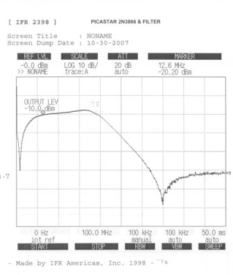 The
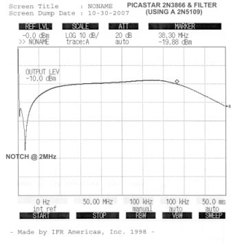
other is 50MHz. Ignore the notch note. It is incorrect. Its simply the low freq.
rolloff of the amp.
The
other is 50MHz. Ignore the notch note. It is incorrect. Its simply the low freq.
rolloff of the amp.
 3rd Nov, 2007, My PICnMIX mounted
in case. That is not the front panel. Another panel is fitted over that one.
Hole to be drilled yet for the opto tuning shaft. (see below)
3rd Nov, 2007, My PICnMIX mounted
in case. That is not the front panel. Another panel is fitted over that one.
Hole to be drilled yet for the opto tuning shaft. (see below)
When you mount the PnM pcb to your front panel, you will need to make sure the spacers you use, allow the displays and keypad to fit behind the panel OK allowing for any display filter you use, also.
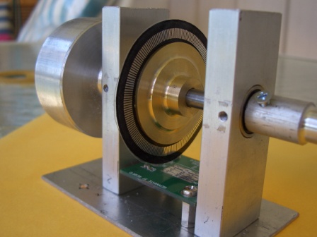
Below is how I mounted my Opto PCB (detached of course from the Butler board). Hole still to be drilled in front panel for the shaft. Knob is a Hamfest/Rally $2 item. The Opto wheel is yet to be sandwiched between the two brass plates. The shaft, from an old potentiometer, runs in some small bearings inserted into the vertical aluminium pieces. The adapter for the knob and the flywheel, retain the bearings which don't need to be a tight fit in the aluminium. The set screws in the side were not needed.
Having access to a lathe helps here of course. Perhaps a local Model Engineers Club can help you out here, if you approach them.
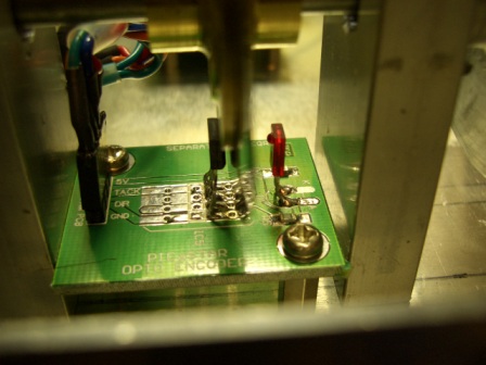
When you mount the Opto PCB section, the LED should be to the FRONT of the radio or your tuning will be reversed ! ie NOT as in the above picture, as I found out. Luckily, the PCB is easily reversed.
The picture above right will give you an idea of the spacing required for correct operation. The Opto detector should be centred in the segments and very close to the opto wheel, which is out of focus in the picture. It is better NOT to use the holes to mount the parts. Bend the leads at right angles and solder them to the tracks. That way you can move them if needed. The LED is further away. I used a SEP8506 LED.
NOTE:- it is not mandatory to use the hole area marked 'area for opto shaft'. You can place the opto shaft anywhere on the front panel you wish. The marked position on the PCB has been kept clear of components and tracks, in case your own selected case is on the narrow side and you need to move the shaft inwards. As you will see above, mine is located to the right of the PCB.
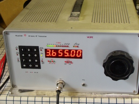 PICASTAR in use on the VK PICASTAR Net.
More Testing, 10th Nov 2007
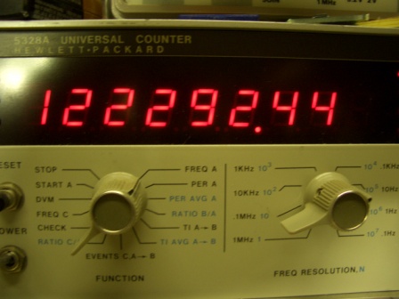
I now have the PICnMIX display board connected up to the Butler board with the DDS carrier board plugged in. All seems to be working as expected. After calibrating the crystal (this time I used a 25MHz crystal removed from an old PC board) I put the unit into signal generator mode and plotted the output level at the 2N5109 output. A call on the STAR chat group got 2 replies so I could compare levels. My measurements are made with a home made AD8307 based level meter so calibration is not known precisely. However, the levels trend track those of Johns quite closely. Above 40MHz, the DDS low pass filter is reducing the level, as expected. (See above graphs)
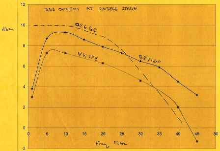
From these results, I believe the PICnMIX and the DDS Carrier are working well.
However, see the STAR Official modifications for a suggestion to improve the high frequency reponse by changing C23 on the 2N3866 stage, by Harold, W4ZCB to 680pF. Yet to be tried on this board. Ref Msg #25245
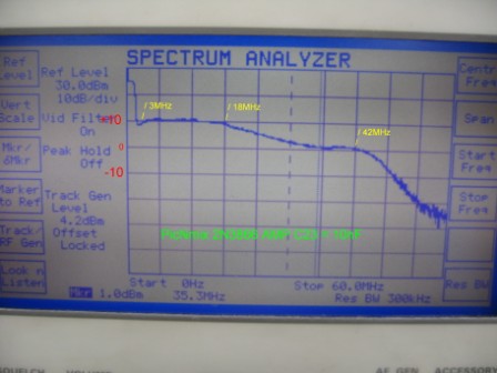 Results
from G8VIQ with C23 =10nF,
27th Nov 2007
Results
from G8VIQ with C23 =10nF,
27th Nov 2007
and with C23 = 680pF Nov 30th 2007
Output level
If you are havoing difficulty geting enough output level, mainly on 10M, then lifting the 56R (R12 ) at the input of the 2N3866 stage, can improve things. This was discussed in the old Yahoo Picastar group when I raised the method.
and...........
Hi Glenn,
just to let you know that lifting the 56 R has had the desired effect. Can´t measure it for lack of suitable gear (frequency is way past the bw of my scope). A rough estimate after comparing traces, though, is 10-20% above previous amplitude (1-2 db). That does not seem much, but was enough to achieve clean rx (ie enough LO drive) on 10m now with the DDS filter in circuit (not possible before).
Mni tnx, gl, 73, Peter Z. (Jan 2009)
ERROR
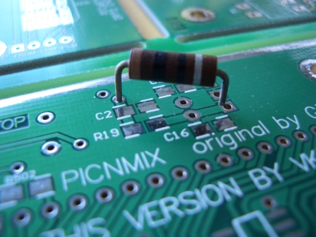
9th Jan 2007 Viv has identified an over dissipation problem in R19. This resistor feeds the 7805 regulator and may overheat. It is best replaced with a 1W axial 10R resistor fitted from the through hole near C2 across to the input pin of the 7805. (near C16) The existing R19 should be removed. On the Version "B" PnM, there is provison for this resistor.
The picture shows an unpopulated PnM PCB, but this is the suggested place to fit the resistor. It should be spaced UP from the PCB by 3 or 4 mm (1/8") for better cooling. Do not force the resistor into the through hole ! If it won't fit, solder it onto an adjacent pad. The picture shows a 0.5W resistor which should be OK but the 1W is preferred.
(21st July, 2008, On the "bonus" set of PnM PCB, Version "B", on Panel #2, this resistor is a through hole part.)
31st Jan 2008, Note that the S'meter will read in reverse with standard Status software. (Msg #28145 & 28146) ie. Right to Left.
This is easily corrected by loading the correct version of the STATUS board code into the PIC. Chirs has passed on to Peter, suitable changes to the source code for this PIC, which can be assembled for Glenn pcb's. ie. correct the readings. No changes to the PCB are required.
Component overlay (pdf) large file 1Mbyte NOTE, for version "B" pcb, BC327's are inserted as per the overlay
Top overlay (more readable) pdf 17th March 08
Bottom overlay (more readable) pdf 17th March 08
7th Jan 08 R73a on above overlay is shown as 1k, SHOULD be 4k7 as per schematic and BOM
Component overlay (pdf) TOP ONLY showing two wire links to be added (see also error above 5th Nov) Panel #1 version only.
26th NOV PICnMIX Schematic (Update_2) 200Kb
8th April, 2008. My schematic shows the 2N3866 output transformer as L100. In Peter's original, this is T1.
PICnMIX schematic (Update_1 ) 31-10-07 1Mbyte Ref only, see Update_2.
by Glenn & Chris