

Last updated on November 18, 2023
home
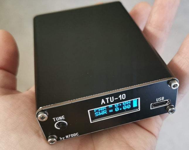
| The ATU-10 by N7DDC: vk3pe's BLOG |
V1.2 - 1.3x BOM updated due to QTY issues in left column...... V1.1 build info. Should cater for V1.2 also NEW May 19th 2023 Test software by N7DDC & How to program the two PIC devices. V1.2 board is a current version but not very latest.. However, see next line. V1.3x are all 0805 versions See it here. 21st Nov 2021 All build info i one pdf file is here. V2.0 is an experimental version using a PIC Evaluation module. Will not be released as yet. Experimental version using Evaluation module UPDATE 27th Aug 2022 I re-worked the original design to add an extra L&C element, to make it an '8x8' ATU for wider tuning range. I have NOT made this PCB but the Gerbers are available in the Group 'Files' area.. Late Aug 2022: David, N7DDC indicated he' may' update the software for this version. David may also do his own 8x8 version at some time incorporating a much better SWR detector chip. So, It would be up to a builder to use my files and test it with David's software if he goes ahead. I just don't have enough parts to do it myself, after building 4 versions already.
|
Background |
N7DDC designed the popular "ATU-100" 100 watt antenna tuning unit (ATU) which is freely available as a kit or even in built up form, from vendors such as eBay, Aliexpress and others. I have built up a couple of these.
The ATU-100 is not suited for outright low current use, as it usd standard relays, so there is always some current drain driving the enabled relays, depending upon how many relays are 'active' switching the L&C's.. LATCHING RELAYS: Recently (June 2021) David (N7DDC) has designed a similar version, but for QRP operation, using latching relays. Using this type of relay results in very low current drain of the unit from internal battery, ideal for Portable operation. (It has also now started to appear on eBay, Aliexpress etc. Beware though, some buyers report problems with operation due to poor soldering etc.) David has also made software to allow his NEW ATU-10 to be used with the IC-705 transceiver. See my IC-705 pages here. For details of David's ATU-10 QRP version of the above, using latching relays. Refer to https://github.com/Dfinitski/ATU-10-10W-QRP-antenna-tuner I built one initially, using Gerbers David supplied on Github. My own build of David's PCB using his Gerber files follows: See also my own re-designed version of David's board, further down. Initially, I used David's PCB Gerber's and had 5 PCB's made by jlcpcb.com™ my usual supplier, in late June 2021. (NOTE I have no financial or any other arrangements with them or any other company for that matter.) I had some issues though actually buying the smaller footprint Micros used on his version.
Getting the other components though is not quite so easy. David has a BOM with some links to Digikey part numbers, but not all. Some parts seem to be fairly unique with no easy alternate parts available. There is some more info available here on this site also.
Building the ATU-10, I found some parts hard to find. David's BOM has Digikey catalog numbers to aid in buying some of the components, but I didn't buy from Digikey due to high shipping costs, at least to VK (Australia). July 10th 2021: I have about 80% of the parts so far, and the PCB's arrived, so I started to assemble a board. Extensive use is made of 0603 sized components which may prove a burden to some builders. (see new notes below on a version using 0805 parts) The two Micro controllers are also smd and very fine pitched parts. The latching relays suggested are actually surface mount parts but the PCB is through hole for them, so the pins have to be straightened to fit. A bit tedious but make sure the pins are fairly straight when you do it.The pins are too short to project through the other side of the PCB so one has to be super careful that they are correctly soldered. A very fine tipped soldering iron is suggested to ensure the solder wicks down into the hole to the relay pins. Another item on the BOM is the battery charger chip, a TP4056. This part is not easy to find, so what I did was to buy a complete charger module on eBay and remove the device from it. There are also two 10uF caps on this board which are not on David's BOM so need to be removed also from the module and used on the ATU-10. However some TP4056 boards may not have these caps. UPDATE: If you search for the TP4056 charger board WITH USB C connector you can also get the correct USB socket to remove and move to this board. As with all parts, I generally err on the side of caution and buy extra parts. Especially with the smd parts, if you need say '10', then order EXTRA parts as you are bound to lose some ! When some parts fall on the floor, it can be impossible to find them again. You will need to do some searching for these parts:- David's BOM has some useful links for these parts.
BIG problem: As most will know there is a huge shortage of IC's at the moment. The hardest to get part currently, seems to be the PIC16F18877-E-MV. I ordered this part from Farnell but it's been put back to delivery in 2022 ! Not holding out much hope but will see if I can find another vendor for it. Digikey, RS-Components, Mouser, UT source, all don't have any. I'm still looking. I had already received the other PIC in this project PIC16F1454, but notice it too has gone onto long lead times at all vendors I could find. Below is comparison of the original PIC specified (small) and the ones I used on my V1.2 board (green) which is described further down the page..
July 15th, 2021 UPDATE:- David has advised that both of the PIC chips used can be found on an "MPLAB Xpress PIC16F18877 Evaluation Board", designated "MICROCHIP DM164142". There still seems to be a few of these available and I ordered from Farnell/Element14 today for arrival in about a week. (Received the Eval module on 22nd July)
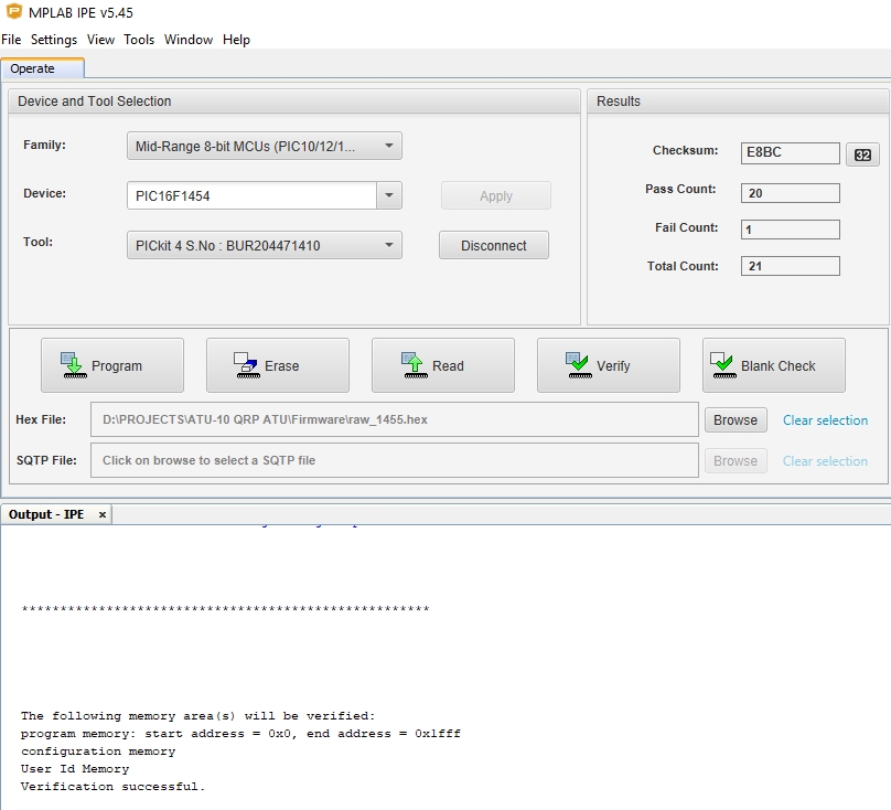
Programming the 'USB' interface Micro (PIC16F1454) is via some pads on the bottom of the PCB. The pads are not marked for function so I traced these back to the device and consulted the data sheet to see what David had in mind here. It's a standard (5pin) 'PIC' programming interface. The second Micro on the board is programmed using this Micro via the USB connector, see David's Github for details. You will need the HEX file and a Pickit4 or similar to program the smaller PIC16F1454 device. I used the App "Microchip's IPE X V5.45. Below you can see the 5 pin header I soldered on temporarily for programming. NOTE:- On my own PCB version (V1.2) I added holes to fit a header for the programmer.
This a screen grab of the IPE X IPE V5.45 programming software.
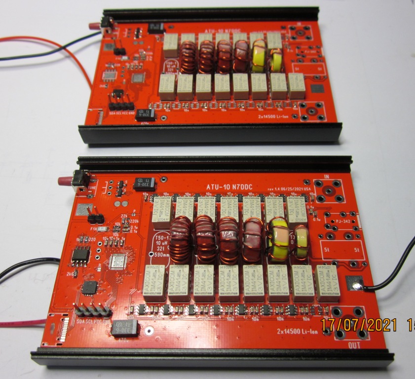
19th July 2021: This is the status of the two boards I have now assembled. As you can see, and from the text above, I am missing some critical parts although hopefully they should arrive in a week or two.
To build this board, I suggest only fitting the capacitors and resistors first, plus the 3v3 regulator. Then (preferably with a variable bench power supply, with current limit) input around 3.7v and check the output of the regulator is indeed 3.3v or very close to it. Slowly increase the external voltage and observe that it's still 3.3v out. Don't fit relays or toroids yet, as they will make it difficult to fit the PIC devices. If anybody is going this way, using the EVAL board and transfer the two PIC's to the ATU-10 PCB, follow the paragraph above first. You need good access around the two chips to enable soldering the PIC devices. Even so it's not easy, these parts were never meant to be hand soldered and the pads are very small, very close pitch and easy to damage the PCB with excessive heat. Even with new parts, it's no walk in the park. I used a VERY fine tip, fine solder (60/40 0.45mm diameter) and the iron set to about 350-375 degrees "C". I also used liquid flux on the PCB to aid solder flow. (you can buy flux pens at low cost to do this) My soldering iron is a very old HAKO® type. 20+ years old actually. I have done one of my two boards and it 'looks' OK when inspecting with a magnifier, but won't know fully until I get a few more missing parts. After careful inspection for shorts and ONLY the PIC16F1454 device fitted, I found the board draws about 2mA from external 5v supply at this stage. (I set the current limit on my supply to about 10mA before connecting it.) Then fitted the PIC16F18877. Double check for shorts between pins etc and then power up the board again. In my case the board now draws about 6mA which seems fair to me. NOTE I haven't proceeded further at this time as I lack some parts still as you can see.
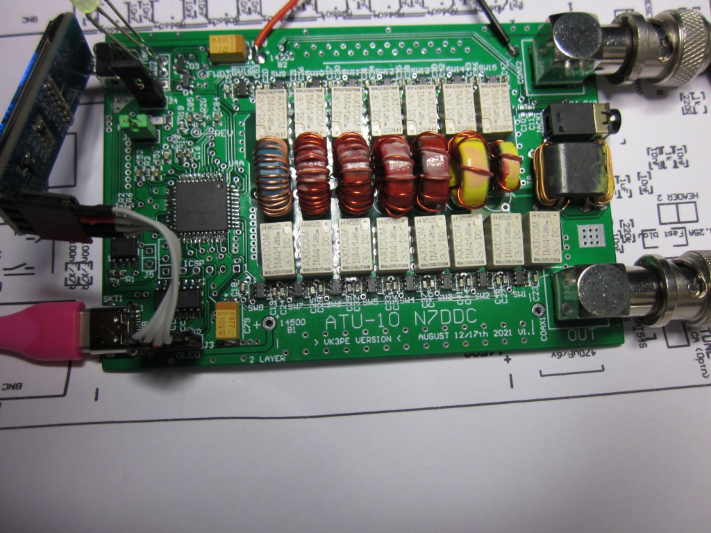
Fit the relays and Toroids last as they make soldering the dual FET's more difficult. Make sure you fit the FET's the right way around, there is a 'dot' on the PCB indicating pin 1 of the devices. MY PCB versions, (below) have ALL OF THE FETS SOLDERED IN THE SAME WAY COMPARED TO David's, BEWARE. The parts themselves also have a dot and it's hard to see. You need to check them with a magnifier or excellent light to see the dot. The PCB (100 x 67mm) has been designed to slide into an aluminium extrusion available from a number of places including eBay. I ordered two and they arrived quickly. The case is quite small at 100 x 71 x 25mm and also contains 2 x 14500 cells that power the ATU. Both cells fit on the ATU-10 PCB.(Not shown below) The PCB is a fairly tight fit into the extrusion.
Updated 25th July 2021:- Once the PIC16F1454 has been programmed as above, the other PIC needs to be programmed. The UCB "C" connector needs to be fitted and a suitable cable to your PC is required. Programming is actually very simple to do.
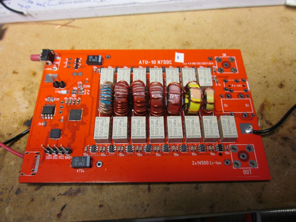
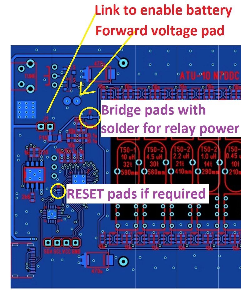
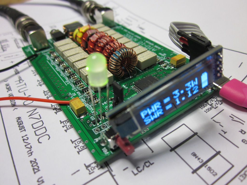
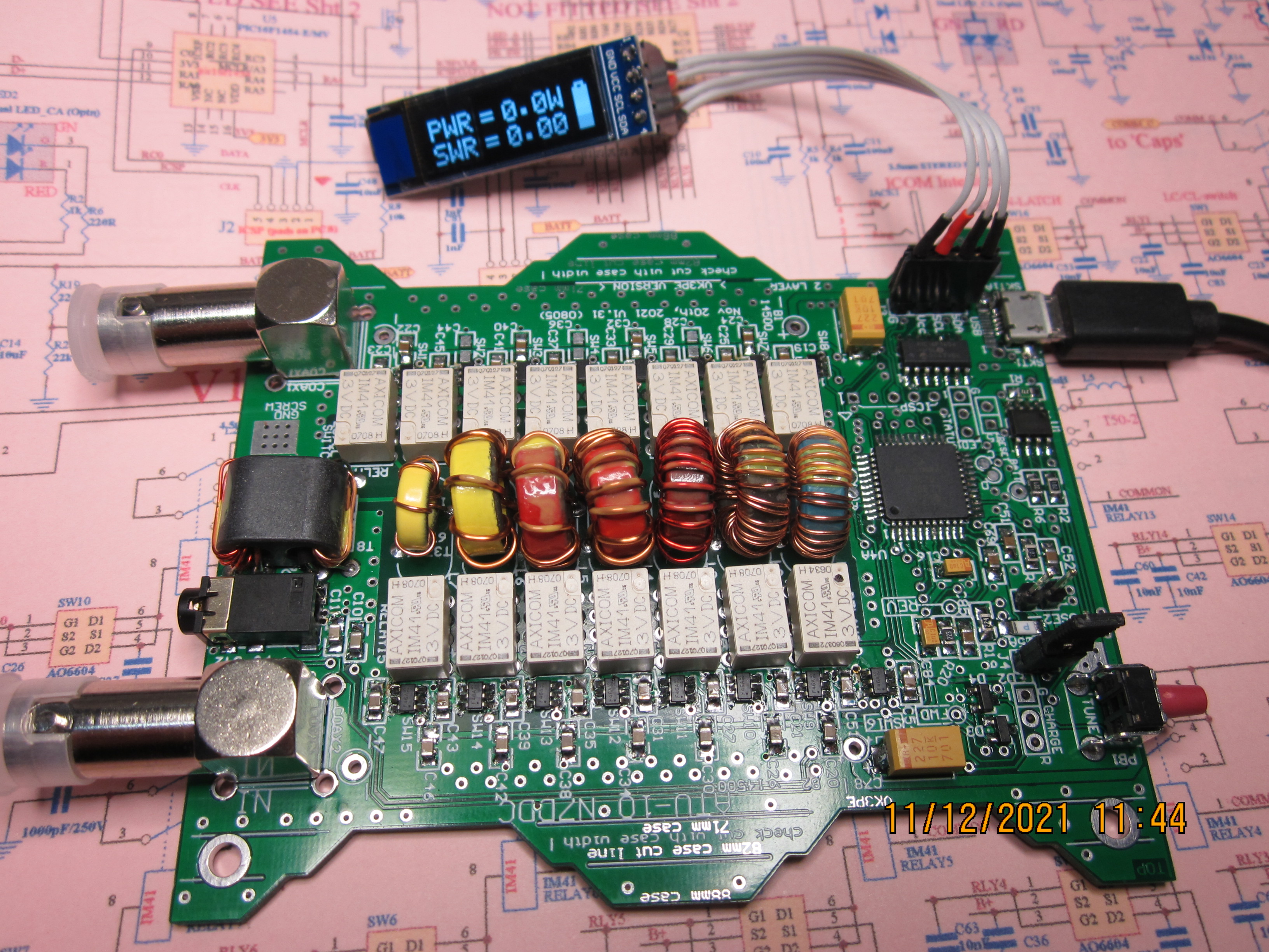
The USB connector has arrived and was used to program the main PIC as detailed above. I wound up the SWR bridge using a BN43-302 balun core since the BN-1502 is not easy to get here in VK. It's a slightly tight fit. Since the BNC connectors have still not arrived I simply soldered some coax onto the connector points, with BNC plugs on the ends for testing. After programming and with the OLED display fitted, you should see the screen showing the version number and then the "PWR = & SWR =" text. If you have gotten this far, the solder pads that supply power to the relays can be bridged with a blob of solder. (the pads are adjacent to the 220R & 220k resistors.
Since the the PCB picture above was taken, I have now fitted the SWR bridge and used some coax cables until the BNC sockets arrived, for testing. At this point I ran a test using my IC-705 as the power source into the "IN" port and connected the "OUT" port to a dummy load for initial testing. Keyed up the IC-705 at 5W and as expected, the ATU-10 showed the power level and an SWR of 1.01. NOTE, in my case PWR showed 4.0Watts although my IC-705 is actually outputting 5W as far as I can tell. The LED above the "TUNE" switch should be flashing slowly, also. Now I connected up a Li-Ion cell. In order for the cell to actually power the ATU-10 you need to link the two "J1" pins. With the USB connected to a PC, the RED LED (It connects to pin 7 of the TP4056) above the TP4056 should be lit, showing the battery is being charged. Once charged, the GREEN LED should light and the RED LED should go off.. Since I don't yet actually have the dual LED's, I only fitted one RED LED as a temporary measure. Update 13th Aug 2021. I received the USB-C connector which was missing in the picture above. Still no BNC connectors but I was able to program the two PIC's and do some tests on the board. So far, all seems OK.
|
Originally, this project could only be built from a bare PCB made with Gerber's from David's GitHub account as detailed above.
My own PCB is version V1.2 and is detailed below.
|
The 'VK3PE' version: One problem with the N7DDC ATU-10 PCB is that it is designed for quite small smd devices, which maybe difficult to solder for some. I did also but eventually soldered the larger device down OK. But I decided to do a 'version' of the PCB of my own, using larger PIC footprint devices, TQFP44 and SOIC14 for the '1454 device. Both far easier to solder. Also, Farnell/Element14 actually had the parts in stock, unlike the original designs devices. This is a screen shot of my re-design, which was ordered on a Chinese supply house and in fact should be here within a few more days and I will report on it. Obviously, the PCB design depends entirely on the Schematic which I traced from N7DDC's PCB. Hopefully it's OK ! We shall see, and I have the original board to compare results with anyway, which is good. I am not supplying Gerber's for this V1.0 PCB, as it has been updated. See below..
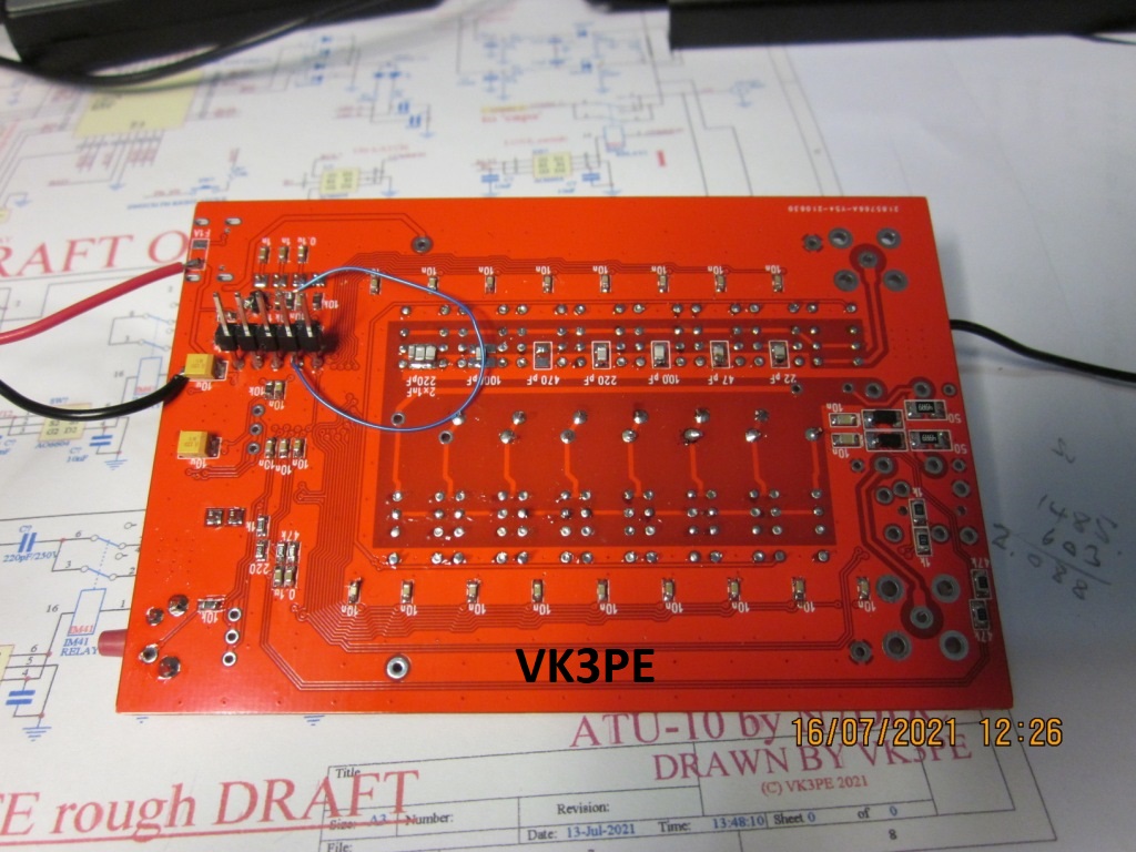
V1.1 31st Aug, 29th Sept, 2021: Version "V1.1" PCB by vk3pe, of new ATU-10 board. (Only a few PCVB's were made) V1.1 is now superceded, but build info is here.>> ZIP File. Right click to save it. May 2023 I have now received the above PCB as Version 1.1 (minor changes to the above) loaded it up and done some preliminary testing. So far it seems to equate well with David's original version as I built originally, near top of this page. V1.2 V1.2 is same Sch as V1.1 but has been designed to fit into 3 different cases, 71mm wide, 82 and 88mm by trimming the edge to the lines marked on it. 1st Oct 2021:- V1.1 & V1.2 use 0603 sized parts as per N7DDC PCB. (Later versions use 0805) V1.2, V1.3 Build information:-
2nd Sept, 2021& updated Dec 2021: David has now made available a Relay Test program on his Github site. I found the earlier version to work better for me. But only his new version is currently on his Github, I think. This solves the problem of not knowing if operation is as expected, (ie the relays are operating) compared to David's original PCB or just to make sure all relays work. As it happens, I discovered a small error in driving Relay '3' which is for the 47pF cap switching. A very easy mod was made to the V1.1 PCB above to correct this so later version also are OK.. (a track cut and short wire link). This was corrected on the PCB version and is now V1.2. (See picture of blank PCB further down the page.) 9th Dec 2021: David has now updated the test program. It now also allows fine tune using the 3.5mm socket connections. See N7DDC Github.
The V1.2 and later blank PCB's with the larger, easier to solder (and obtain) PIC devices, is available from Kees, K5BCQ and some others in the ATU100 Group. Refer to the ATU-100 Groups.io group for details. See picture below also. V1.2 differs slightly from that shown above (V1.1) as it has been widened with "wings" to allow fitting into three different case styles, the original 71mm wide used by N7DDC and shown above and also either 82 or 88mm wide cases. Simply by trimming to suit on the cut lines. All cases vary in price, the 82mm was about half the cost of the 71mm case when I purchased one recently. All of the documents referring to V1.1 apply equally to V1.2.
Trim slightly wider initially, and file down to make a good fit into the case chosen.
ABOVE:- Here's a comparison of the 71mm (top) and 82mm wide cases. The 82mm is a few mm higher also, both are 100mm long.
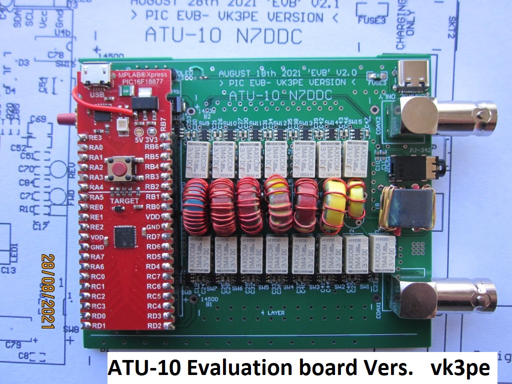
An alternate idea, to avoid soldering and buying the original (small) PIC devices:- An experiment here to use the Microchip "Evaluation module":-II decided to try out the Microchip Evaluation Board in a version of the above. It is functionally equivalent to using two separate PIC devices. It eliminates soldering the PIC devices entirely. A side benefit is that the Eval board seems to be much easier to purchase than the PIC devices themselves, although more expensive than two PIC's. . Another benefit is that the PIC16F1454 is pre-programmed so no Pickit3 or similar is required at all. The PCB I made is designed to fit into either of two extruded aluminium cases available on eBay. eg the 100 x 82 x 27mm size. Or 100 x 88 x 38mm. It is a little wider than the PCBs above as the Eval Module is quite long as you can see below.. Due to the difficult routing of this version, the PCB is now a 4 layer board, compared to the other versions which are 2 layer. I am still testing this version, but so far it seems OK.
The white line on the PCB is a "cut line" to trim the PCB to suit a smaller case. I'm waiting on delivery of the 82mm wide case, for checking. Please note that this information is presented as-is and is thus subject to possible errors and omissions. (The Schematic was traced from N7DDC's original PCB and adapted to use the Evaluation module..)
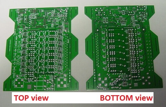
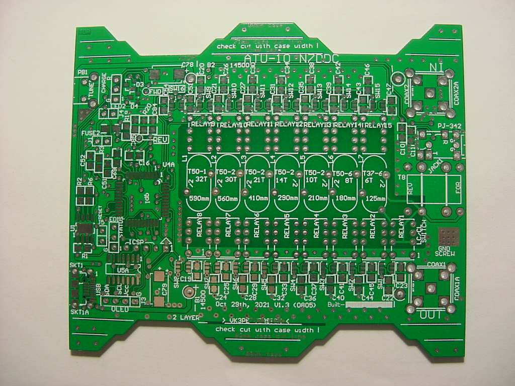
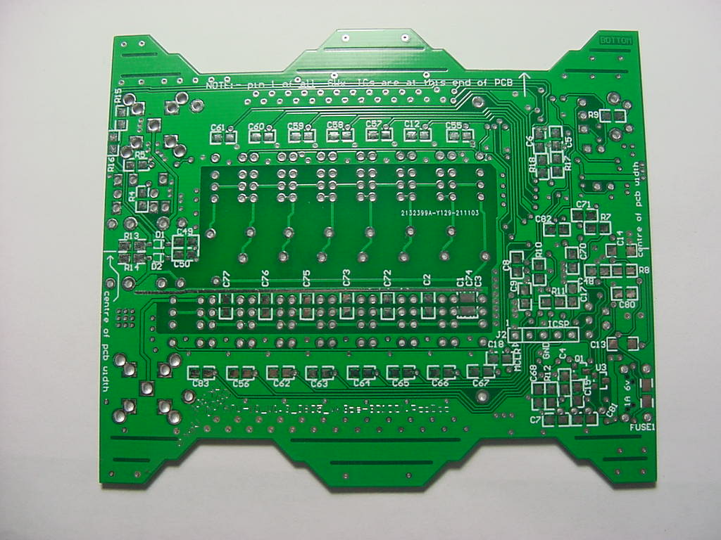
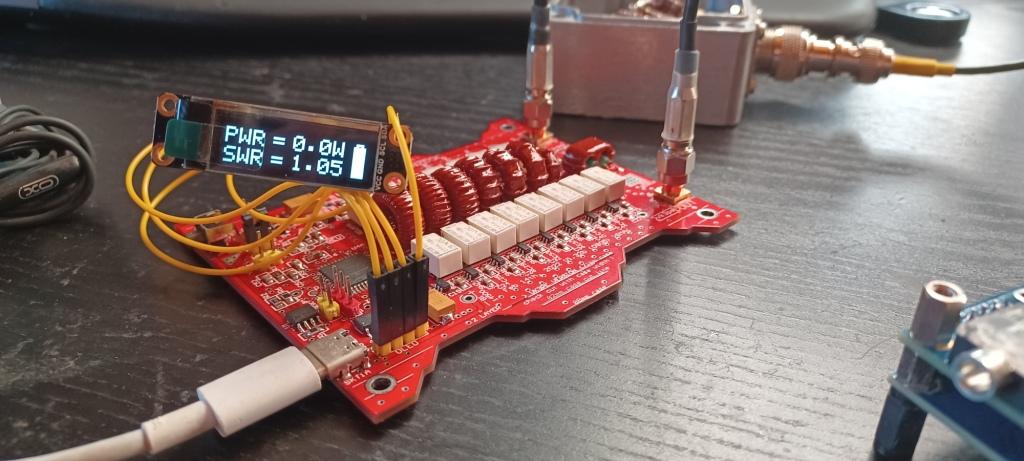
21st Nov 2021:- V1.3 and later -->> Larger components, ie moving from 0603 to 0805 parts, easier to solder etc. I have now finished designing a new version of the board, changing all the 0603 components on the V1.2 board to 0805 parts, making it easier to assemble. Especially for those like me of the 'older' generation with bad eyesight, trembling hands etc. As you can see from the pictures below, the BNC sockets now have extra ground holes spaced at 10.05mm (standard is 6.6mm) which may suit alternate BNC connectors. Due to some interference, the 'OUT" BNC connector had to me moved slightly downwards. The board version moves from V1.2 to V1.31. The V1.2 with 0603 is still current though. As before, the PCB will fit 3 different case sizes. Here's some pictures of V1.3, (top & bottom) almost identical to V1.31 which is on the way. Just minor changes for V1.31. One is the addition of 4 mounting holes to fit the PCB into a case which doesn't have the slide in grooves. Click pictures for larger size.
More later........... This web page was created by VK3PE on July 16th 2021. Last updated on November 18, 2023 Please note this web page is a summary of what I did, it may not work for you. Some items or text on this page may refer to ™ or ® companies. I have NO commercial affiliation of any kind, with any mentioned Company or any other for that matter..
|
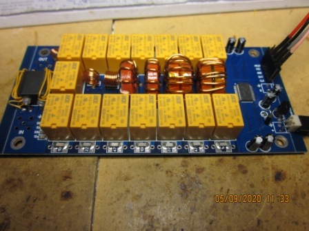
 Picture borrowed from David's Github.
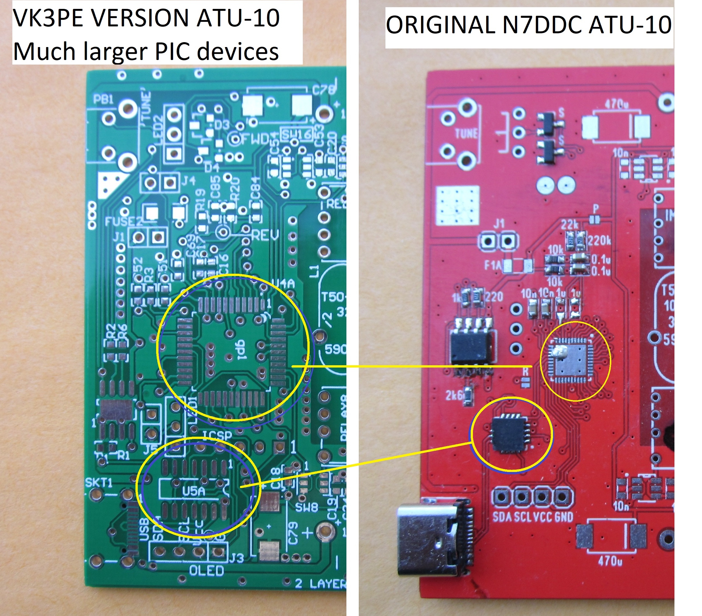
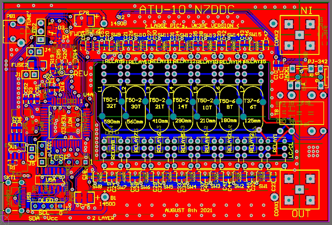
 V1.2 PCB showing how it maybe trimmed to suit 3 case widths. As-is for the 88mm wide case, trim to 1st lines for 82mm and trim all tabs off for 71mm case.
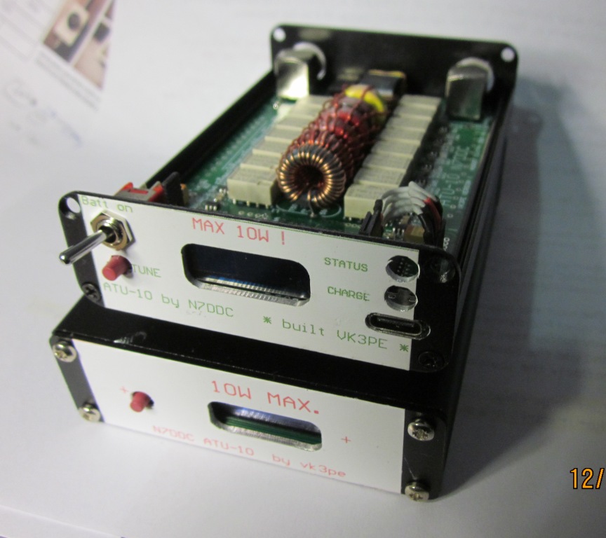
 The Evaluation module is on the left side (red) and plugs into my V2.0 PCB.
 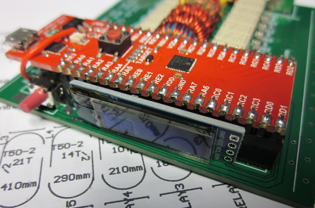 Display position. (Not yet wired in)